When developing a product with a custom LCD module, successful integration goes far beyond simply matching the interface type. Just because both the mainboard and the display use LVDS, eDP, MIPI, RGB, HDMI, or DP does not guarantee a correct image. Signal mapping is where many custom LCD projects encounter time-consuming problems such as wrong colors, split screens, shifted images, flicker, or no image at all.
Signal mapping is a system-level challenge that requires the mainboard output, controller board, cable, interface configuration, timing, color format, and LCD panel input requirements to be aligned as one complete signal chain. A correct interface name alone does not guarantee a correct display result.
In custom LCD module projects, many apparent display abnormalities are not caused by a defective panel. The module may be electrically functional, but the image data may arrive in a format, order, timing, or lane configuration that the LCD panel cannot interpret correctly. This is why signal mapping should be reviewed before assuming that the display sample itself has failed.
This article explains common signal mapping issues in custom LCD module projects, why non-standard displays increase mapping risk1, how different interfaces require different checks, and how project teams can prevent these problems before sampling or production.
Signal Mapping Is More Than Interface Matching
A common misconception in display integration is that if the interface types match, the display should work. In reality, the interface name is only the first checkpoint. Within the same interface type, there can still be differences in pinout, lane order, color format, bit depth, resolution timing, controller settings, and panel initialization.
True compatibility depends on a precise match of pinout, lane order, channel mapping, color format, bit depth, resolution timing, scan direction, and controller configuration. Signal mapping must be treated as a system-level validation, not only an interface-level check.
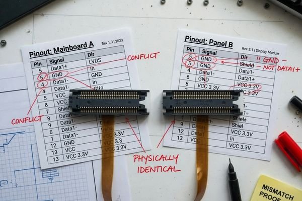
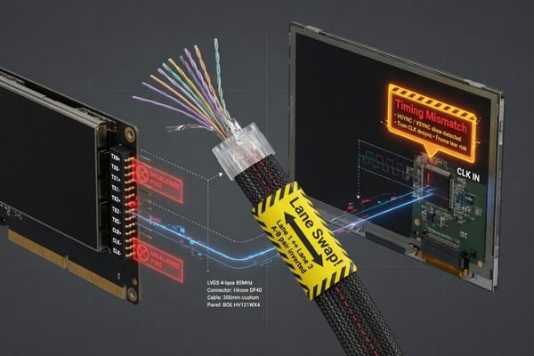
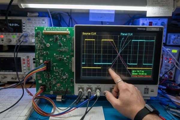
In project reviews, the problem often lies in subtle but critical differences. A mainboard may output data using one LVDS mapping format, while the panel expects another. Both sides may be described as LVDS, but the data-to-pin mapping can still be different. The result may be incorrect colors, distorted image data, or an unstable display.
The same applies to color order, bit depth, timing, and scan direction. A mismatch between RGB and BGR order2 can cause incorrect color display. Incorrect timing can shift or crop the image. Wrong scan direction can make the image appear mirrored or rotated. For this reason, signal mapping should be checked across the source device, controller board, cable, and LCD panel together.
Common Display Symptoms Caused by Signal Mapping Problems
Signal mapping problems often appear as visible display abnormalities rather than obvious hardware failures. This can be confusing during sample bring-up because the first reaction may be to suspect a defective LCD panel. In many cases, however, the display is receiving a signal that does not match its expected format.
Display issues such as wrong colors, split image, duplicated content, shifted display area, flicker, cropped image, partial display, or no image are often caused by signal mapping errors. These symptoms usually point to a mismatch in timing, color order, lane mapping, pinout, scan direction, or controller configuration.
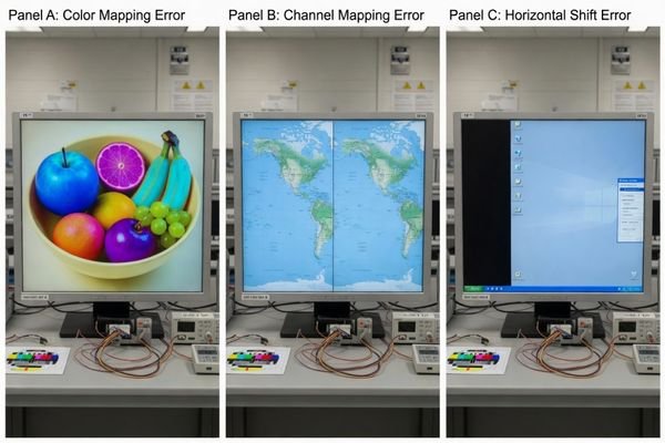
The following table connects common display symptoms with likely signal mapping causes.
| Display Symptom | Possible Signal Mapping Cause |
|---|---|
| Wrong colors | RGB/BGR order, bit depth, LVDS mapping, color format mismatch |
| Split or duplicated image | LVDS channel mapping, scaler configuration, timing mismatch |
| Shifted image | Active area, sync, porch, or timing setting issue |
| No image | Pinout mismatch, power sequence issue, unsupported interface |
| Flicker or unstable image | Timing instability, signal configuration, cable issue |
| Cropped image | Resolution mismatch or scaler mapping error |
| Mirrored or rotated image | Scan direction or controller setting mismatch |
| Partial display | Lane/channel mismatch or unsupported panel configuration |
Recognizing these symptoms as possible signal mapping issues can reduce unnecessary troubleshooting time. Before assuming the LCD panel is defective, the project team should review the interface, timing, pinout, controller configuration, cable design, and system output together.
For projects involving non-standard outputs, interface conversion, or controller adaptation, display interface customization can help define the correct signal path before further debugging.
Why Non-Standard LCD Modules Increase Mapping Risk
Signal mapping matters in any display integration project, but the risk increases when the display format moves away from standard screen formats. Bar-type displays, ultra-wide displays, square displays, portrait displays, and custom-shaped LCD modules often require more careful review because they may use unusual resolutions, special timing, or customized controller settings.
The more a display format deviates from standard 16:9 or 4:3 screens, the more important signal mapping review becomes. Non-standard LCD modules often require review of native resolution, timing, scaler configuration, mainboard output, cable direction, and controller board adaptation.
The issue is not that non-standard LCD modules are inherently unstable. The risk comes from the fact that their resolution, timing, active area, orientation, or cable direction may not match the default output settings of standard mainboards or controller boards.
For example, a 1920×360 bar-type display may not be directly supported by a mainboard configured for standard 1920×1080 output. The correct solution depends on whether the mainboard can output the native resolution directly, whether a controller or scaler board is needed, and whether the UI can be mapped without distortion.
Non-standard modules may also involve special FPC cable direction, unique pinout requirements, rotated UI layouts, or customized power sequencing. When evaluating bar-type, ultra-wide, square, vertical, or custom-shaped modules, it is useful to compare available display module types before deciding whether a standard module, modified structure, or fully customized configuration is required.
Interface Type Changes the Mapping Review
Different display interfaces have different signal mapping risks. The review process for LVDS is not the same as the review process for eDP, MIPI DSI, RGB, HDMI, or DP. Each interface has its own critical parameters that must be checked before the display configuration is locked.
Each display interface has its own mapping checkpoints. LVDS projects require review of channel and format mapping; eDP projects require lane count, link rate, EDID, and timing confirmation; MIPI DSI projects require lane configuration, packet format, and initialization commands.
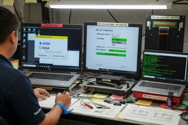
For LVDS projects, key checks usually include JEIDA versus VESA mapping format, single-channel versus dual-channel configuration, 6-bit versus 8-bit color depth, odd/even pixel mapping, and pinout alignment. A mismatch in any of these areas can lead to wrong colors, split images, or unstable display output.
For eDP projects, the review should include lane count, link rate, EDID, resolution timing, and panel compatibility. eDP often provides a more structured link negotiation process, but it still requires confirmation that the mainboard output and panel input requirements are aligned.
For MIPI DSI projects, the review usually includes lane count, packet format, panel initialization commands, power sequence, and panel-specific configuration. MIPI-based displays can be highly panel-specific, so relying only on the interface name is not enough.
For parallel RGB interfaces, pin assignment, sync signals, clock polarity, and color depth must all be checked carefully. For HDMI or DP controller solutions, the focus often shifts to scaler configuration, EDID programming, and output timing. In projects where interface matching is uncertain, display interface customization should be reviewed before sampling.
Hardware, Firmware, and Software Must Work Together
Diagnosing signal mapping issues is rarely a one-dimensional task. Some problems can be corrected through controller firmware, timing settings, EDID configuration, scan direction, or software output settings. Other problems require changes to the cable, connector, PCB, controller board, or LCD module structure.
A reliable diagnosis requires hardware, firmware, and software to be reviewed together. Some mapping problems can be corrected through firmware or timing configuration, while hardware-related issues such as wrong pinout, unsupported interface, or insufficient lane count may require physical design changes.
A color order issue, for example, may be corrected by changing RGB/BGR settings in the controller firmware or software driver. A shifted image may be improved by adjusting timing parameters, active area settings, porch values, or scaler configuration. A mirrored or rotated image may be corrected through scan direction or controller configuration.
However, not every mapping problem can be solved through software. If the cable pinout is wrong, the panel interface is unsupported, the lane count is insufficient, or the controller board does not support the required resolution and timing, a hardware change may be required.
This distinction is important because it affects project schedule and cost. Treating a hardware limitation as a software issue can waste debugging time.3 Treating a firmware setting issue as a hardware defect can lead to unnecessary redesign. A structured review should identify where the mismatch occurs in the signal chain before deciding how to fix it.
How to Prevent Signal Mapping Issues Before Sampling
The best way to handle signal mapping issues is to prevent them before the first sample is built. Once hardware has already been produced, mapping problems can lead to repeated debugging, cable changes, controller board adjustments, or even redesign of the display module configuration.
Signal mapping validation should be a design-stage checkpoint, not only a troubleshooting step after samples are built. Before sampling, the project team should confirm the panel datasheet, native resolution, timing table, interface type, pinout, mainboard output, lane configuration, power sequence, controller board requirements, and cable direction.
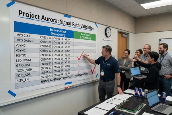
In custom LCD module projects, our engineering review usually starts by comparing the source side and panel side requirements. This includes the mainboard output capability, panel datasheet, interface specification, pinout table, timing parameters, color depth, lane mapping, cable design, power sequence, and display orientation.
This review helps identify possible conflicts before they become sample-level problems. For example, the mainboard may support the interface type but not the required native resolution. A controller board may support the resolution but require firmware adjustment. A cable may fit mechanically but have the wrong pin sequence or FPC direction.
Before a custom LCD module configuration is locked, it is better to discuss your custom display project and review the signal path as a complete system. Early validation can reduce debugging time, redesign risk, and production delays.
Signal Mapping Checklist for Custom LCD Projects
A structured checklist helps turn unclear display problems into reviewable engineering items. Instead of describing the issue only as “wrong image” or “screen not working,” the team can check specific parameters one by one and identify where the signal chain is not aligned.
A signal mapping checklist translates vague display requirements into concrete engineering items. It helps verify whether the mapping issue comes from panel input requirements, mainboard output, controller configuration, cable design, timing, color format, power sequence, or display orientation.
Before confirming a custom LCD module design, project teams should review these questions:
- What is the LCD panel’s exact native resolution?
- What interface does the LCD panel require?
- What interface does the mainboard output?
- Is the output format directly supported, or is a controller board required?
- Have the mainboard connector, cable, and display FPC pinouts been confirmed?
- What are the required timing parameters, including H-total, V-total, porch values, sync, and clock frequency?
- What color depth and color order are used by the source and the panel?
- Has LVDS, eDP, or MIPI lane mapping been confirmed?
- Is JEIDA/VESA mapping relevant for the LVDS configuration?
- Is EDID required or configured for the controller or mainboard?
- Is the power-up and power-down sequence compatible with the panel?
- Is the display orientation, scan direction, or rotation requirement fixed?
- What sample test conditions will be used during bring-up?
This checklist is especially useful when several teams are involved, such as the mainboard supplier, LCD module supplier, cable supplier, controller board supplier, and equipment manufacturer. Clear documentation reduces the risk of each side assuming that another party has already confirmed the mapping details.4
When to Request Engineering Review for Signal Mapping
Some simple LCD integrations can be handled with standard module documentation and a straightforward interface match. However, an engineering review becomes important when the project includes non-standard resolution, interface conversion, controller board adaptation, special cable design, new mainboard output, or any display abnormality during bring-up.
Engineering review is recommended when a project involves non-standard resolution, bar-type displays, ultra-wide displays, custom-shaped panels, interface conversion, controller board adaptation, special cable design, or image abnormalities during testing. A structured review helps identify whether the issue comes from timing, pinout, lane mapping, firmware, or hardware limitations.
In practice, the need for engineering review often appears when several risks overlap. A project may involve a non-standard LCD resolution, a new mainboard, a custom FPC cable, and a controller board at the same time. In that situation, checking only one part of the system is not enough.
The review should determine whether the problem is caused by timing settings, pinout mismatch, lane/channel mapping, color format, firmware configuration, power sequence, cable direction, or hardware limitations. It should also identify whether the issue can be solved through settings, firmware, cable modification, controller board changes, or a different module structure.
For projects that require deeper integration across panel selection, interface mapping, controller configuration, and long-term module planning, custom LCD module engineering is usually the most practical next step.
Signal Mapping Issues FAQ
What is signal mapping in an LCD module?
Signal mapping defines how image data, color information, timing signals, lanes, channels, and control signals are transferred from the mainboard or controller board to the LCD panel.
Why does an LCD show wrong colors?
Wrong colors may be caused by RGB/BGR order mismatch, bit depth mismatch, incorrect LVDS mapping format, color format settings, or controller configuration errors.
Why does a custom LCD show a split or shifted image?
Split or shifted images are often related to resolution timing, active area settings, sync parameters, LVDS channel mapping, scaler configuration, or unsupported output format.
Can signal mapping problems be fixed by software?
Some issues can be corrected through firmware, timing settings, color order, scan direction, scaler configuration, or EDID adjustment. Hardware-related issues such as wrong pinout, insufficient lane count, unsupported interface, or cable mismatch may require board, cable, or module changes.
What information is needed before mapping a custom LCD module?
Important information includes the panel datasheet, native resolution, timing table, interface type, pinout, mainboard output, color depth, lane configuration, controller board details, power sequence, cable design, and display orientation.
Conclusion
Signal mapping issues in custom LCD modules should be treated as system-level integration risks, not isolated display defects. A successful display bring-up depends on the alignment of the mainboard output, controller board, cable, interface configuration, timing, color format, power sequence, and LCD panel input requirements.
Before a custom LCD module configuration is locked, the signal path should be reviewed from end to end. If your project involves non-standard resolution, interface conversion, controller board adaptation, custom cable design, or image abnormalities during testing, custom LCD module engineering can help reduce debugging risk and support a smoother path to production.
→ Start your custom display project
✉️ info@lcdmodulepro.com
🌐 https://lcdmodulepro.com/
-
"Custom LCD Display Modules | Tailored Size, Interface", https://www.displaymodule.com/de/blogs/knowledge/custom-lcd-display-modules-tailored-size-interface?srsltid=AfmBOor0Ol5ukRU21YBZj9QmFNmXafztd2cTIPyj5RKMJdTa8y6hc_TV. Technical guidelines note that deviations from standard interface specifications introduce additional signal‐routing and timing complexities, raising the likelihood of mapping faults in custom LCD modules. Evidence role: expert_consensus; source type: research. Supports: Non-standard displays increase mapping risk. Scope note: Focuses on common interface standards and may not cover all proprietary implementations. ↩
-
"Why do some graphics libraries use BGR instead of RGB color …", https://www.reddit.com/r/computergraphics/comments/1fzzt84/why_do_some_graphics_libraries_use_bgr_instead_of/. Explains that swapping the sequence of color channels from RGB to BGR leads to swapped or incorrect color output on displays. Evidence role: mechanism; source type: encyclopedia. Supports: A mismatch between RGB and BGR order can cause incorrect color display.. Scope note: General explanation; some display controllers automatically reorder channels. ↩
-
"The Leader in Embedded Software Development Tools", https://www.ghs.com/ToolsLeader.html. Case studies in embedded systems development indicate that misdiagnosing hardware limitations as software defects can extend debugging phases by several weeks. Evidence role: case_reference; source type: paper. Supports: Treating a hardware limitation as a software issue can waste debugging time.. Scope note: Specific durations vary by project complexity and team expertise. ↩
-
"The Impact of Structured and Standardized Documentation on …", https://pmc.ncbi.nlm.nih.gov/articles/PMC9135789/. Standards such as ISO/IEC/IEEE 15288 emphasize that comprehensive interface documentation mitigates assumption gaps and integration risks among collaborating hardware teams. Evidence role: expert_consensus; source type: institution. Supports: Clear documentation reduces the risk of each side assuming that another party has already confirmed the mapping details.. Scope note: Applicability may vary with team compliance to documentation processes. ↩